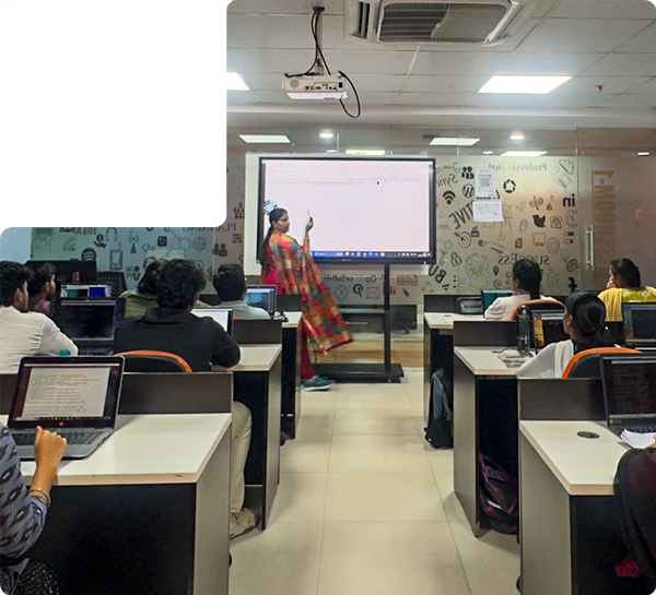
Introducing S.I.T.

A VLSI training institute with over 8 years of experience, dedicated to preparing engineers for careers in semiconductor design.

The institute offers specialized training in key semiconductor domains including
Physical Design, Design Verification, & Analog Layout.

The learning approach focuses on helping engineering graduates move beyond academic theory and develop practical understanding of semiconductor design workflows used in industry.

Through domain-focused training and structured learning, Sumedha Institute of Technology aims to help students build strong foundations for long-term careers in semiconductor engineering.


15+
Average Faculty Experience Years
200+
Recruitment
Partners
250+
Placement
Drives
2000+
Placed
Across

img
shape

Why Semiconductor Careers Matter Today

img

India contributes 20% of global chip design workforce.

Surge in high-paying core semiconductor roles.

img

Semiconductors power modern technology systems — from smartphones and artificial intelligence to automotive electronics and cloud infrastructure.

As electronics continue to evolve, the demand for engineers with specialized semiconductor design skills has increased significantly. Companies developing modern chips require engineers who understand domains such as:
Physical Design, Design Verification, & Analog Layout.

For engineering graduates interested in working at the core of modern technology, semiconductor design offers opportunities to build specialized expertise within a rapidly evolving industry.

Choose Your Domain

image-1
Physical Design

Physical Design engineers transform digital circuit designs into manufacturable chip layouts. This domain involves floorplanning, placement, routing, and timing optimisation before chip fabrication.


Know More
image-1
Design Verification

Design Verification ensures that chip designs function correctly before manufacturing. Engineers build verification environments and validate digital designs using structured verification methodologies.


Know More
image-1
Analog Layout

Analog Layout engineers convert circuit schematics into precise layouts while maintaining signal integrity and performance for analog circuits. This requires attention to precision, matching & layout optimization.


Know More

Industry Aligned Learning With Practical Exposure

Sumedha Institute of Technology focuses on building domain understanding through structured learning and practical exposure.

Students work through industry-inspired design scenarios that require them to investigate problems, analyse results, identify root causes, make engineering decisions, implement solutions, and validate outcomes. This helps develop practical problem-solving skills beyond predefined exercises.

Students also gain access to S.I.T.'s own AI-powered solution during their learning journey, using AI to support problem solving, debugging, analysis, automation, and engineering tasks while learning to evaluate and validate AI-generated outputs.

As part of the training, all students undergo a 6-month internship exposure, allowing them to experience practical semiconductor design workflows and engineering environments.

img

Learn from Industry Experienced Faculty

img

One of S.I.T.'s key strengths is its faculty team, which includes professionals with industry experience across semiconductor and VLSI domains.

Faculty members bring experience from leading semiconductor and technology environments, including organisations such as Intel, NVIDIA, AMD, Synopsys, Marvel and Intersil.

Having worked within engineering teams and semiconductor design environments, these faculty members bring practical insights that help students understand how concepts are applied beyond the classroom.

Students benefit from exposure to real-world workflows, project experiences, and engineering practices that are commonly encountered within semiconductor organisations.

This industry perspective helps bridge the gap between academic learning and professional expectations.


Meet Our Faculty

Tools Used in Semiconductor Design

Modern semiconductor development relies on specialised design environments used by chip engineering teams.

Training at S.I.T. introduces students to semiconductor design workflows and environments commonly used in industry, including ecosystems from major semiconductor tool ecosystems such as:

img

Exposure to these tools alongside domain concepts helps students understand how semiconductor engineering teams operate.

img

Who Should Consider S.I.T. Training

Engineering-icon
Final-year engineering students

Interested in semiconductor
design

Engineering-icon
Recent graduates

Seeking specialized VLSI domain training

Engineering-icon
Professionals

Looking to transition into semiconductor careers

The programs focus on helping students build domain clarity and practical understanding of semiconductor design workflows.

Why S.I.T.

img
Domain-Focused Learning

Training is structured around specialized semiconductor design domains rather than generic electronics training.

img
Industry Experienced Faculty

Students learn from faculty with semiconductor industry experience and practical domain expertise.

img
Practical Exposure

Students gain exposure to domain concepts, tools, and design flows used in semiconductor development.

img
Career-Oriented Approach

The objective is to help engineers prepare for roles within semiconductor design teams.

Career Pathways

Learn About Semiconductor Design

Training at S.I.T. prepares students for specialised roles within semiconductor design teams.

Graduates typically begin in roles such as:

  • Physical Design Engineer
  • Design Verification Engineer
  • Analog Layout Engineer

These roles contribute to different stages of semiconductor chip development, from validating design functionality to implementing manufacturable layouts.

As engineers gain experience, they may progress into advanced roles involving design optimisation, complex system-level understanding, and leadership within semiconductor projects.

S.I.T. training is designed to help students build the foundational knowledge required to begin and grow within semiconductor design careers.

Placement Highlights

Prasanna Lakshmi

Capgemini

Manohar Reddy

AMD

Sasi Kala

HCL

Manohar

Wipro

Kamala

Digicomm Semiconductor

Kusuma

Chipex Technologies

Recruitment Partners

AMD Logo
Advanced Micro Devices
Cadence
Cadence
Capgemini
Capgemini
Chipex
Chipex
HCL
HCL
Intel
Intel
Micron
Micron
Nvidia
Nvidia
Qualcomm
Qualcomm
Siemens
Siemens
Synopsys
Synopsys
Wipro
Wipro

Not Sure Which Domain to Choose?

Many students exploring VLSI training are unsure which semiconductor domain aligns best with their interests.

Each domain within semiconductor design focuses on a different stage of chip development and requires a different type of problem-solving approach.

  • Physical Design focuses on implementation and optimisation of chip layouts
  • Design Verification focuses on validating digital functionality and identifying design issues
  • Analog Layout focuses on precision-based implementation of analog circuit designs

Understanding these differences can help you make a more informed decision.

S.I.T. advisors can help you evaluate your background, interests, and career goals to guide you toward the most suitable domain.


Know More
img

Learn About Semiconductor Design

img

Building a career in semiconductor design requires understanding how chip development works and how different engineering roles contribute to the process.

The S.I.T. knowledge section explores topics such as semiconductor design workflows, domain comparisons, and career pathways in VLSI.

Students can learn about how chips are designed, how different domains interact, and what skills are required to build a career in semiconductor engineering.

This section is designed to help students gain clarity before choosing a training path.


Explore Learning Resources

Scholarships & Pay After Placement

S.I.T. recognises that financial considerations play an important role when students choose specialised training programs. To support deserving candidates, structured financial support options are offered based on eligibility and evaluation.

These options are designed to make quality semiconductor training more accessible while ensuring that selection remains aligned with student readiness and program expectations.

Selected candidates may benefit from:

  • Merit-based scholarships based on academic performance and overall evaluation
  • Pay After Placement opportunities offered through a structured selection process

These options are designed to support students while maintaining strong training standards, commitment, and alignment with semiconductor career pathways.


Learn More
Learn About Semiconductor Design

Frequently Asked Questions

VLSI training focuses on semiconductor design domains such as design verification, physical design, and analog layout used in integrated circuit development.

The choice depends on your interests and career goals. Some domains focus on digital verification, while others focus on physical implementation or analog circuit layout.

Semiconductor design remains a specialised engineering field with strong demand as modern electronics continue to evolve.