Physical Design is a critical stage in semiconductor chip development where digital circuit designs are transformed into manufacturable chip layouts.
The Physical Design course at Sumedha Institute of Technology (S.I.T.) introduces students to the concepts, workflows, and tools used in physical implementation of integrated circuits.
This training is designed to help engineering graduates understand how digital designs move from logical representation to physical silicon implementation.
The Physical Design course at S.I.T. helps students build domain knowledge required for physical implementation roles within semiconductor design teams.
Physical Design (Backend VLSI)
Implementation of digital chip designs into manufacturable semiconductor layouts.
Domain focused learning with practical exposure to semiconductor design workflows.
6 months.
All students undergo a 6-months internship exposure as part of the training.
Engineering graduates and professionals interested in semiconductor design careers. Career Roles
Physical Design Engineer | Backend Design Engineer | Implementation Engineer
Physical Design refers to the process of converting digital circuit designs into a physical layout that can be manufactured as a semiconductor chip.
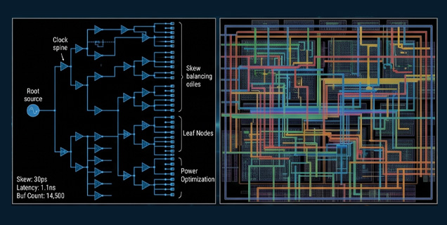
This stage involves several steps including floorplanning, placement, clock tree synthesis, routing, and timing optimisation.
Physical Design engineers ensure that the design meets performance, power, and area requirements while remaining manufacturable.
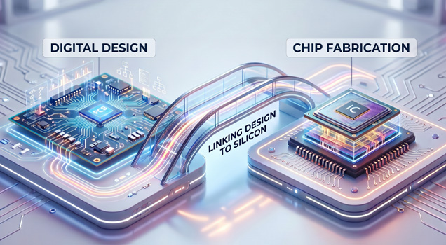
In semiconductor design workflows, Physical Design bridges the gap between digital design and chip fabrication.
Once digital functionality is defined and verified, Physical Design engineers prepare the layout that will ultimately be fabricated as silicon.
Their work ensures that the chip design is physically feasible and meets performance targets.
Students training in Physical Design typically build understanding in areas such as:
The training combines conceptual understanding with scenario-based problem solving, where students investigate Physical Design challenges, analyse implementation results, identify root causes, make engineering decisions, apply solutions, and validate outcomes.
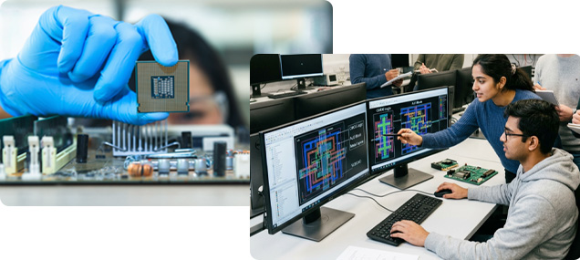
Physical Design engineers use specialised tools to implement chip layouts and analyse design constraints.
Training introduces students to semiconductor design environments commonly used in industry, including design environments from major semiconductor tool ecosystems such as:
Exposure to these environments helps students understand how physical implementation workflows operate in semiconductor design teams.
Alongside industry-relevant design environments, students gain access to S.I.T.'s own AI-powered solution to support problem solving, debugging, analysis, automation, and engineering tasks while learning to evaluate and validate AI-generated outputs.
Training is delivered by faculty members with experience in semiconductor and VLSI environments.
Having worked on semiconductor implementation workflows and design projects, these faculty members bring practical perspectives that help students understand how Physical Design concepts are applied within engineering teams.
Students also undergo a 6-months internship exposure, helping them connect classroom learning with real engineering environments and semiconductor design workflows.
This combination of industry-guided learning and practical exposure helps bridge the gap between academic understanding and professional expectations.
Physical Design training prepares engineers for roles involved in implementing and optimising digital chip designs before semiconductor fabrication.
Entry-level roles typically include:
Engineers working in Physical Design often progress into more advanced roles as they gain experience in chip implementation and design optimisation.
Typical career progression may include:
These roles contribute to different stages of semiconductor chip implementation within design teams.
Manohar Reddy
Gunavardhini
Mirza Hasnain Mehti
Amrutha
Visweswara Sai
Eshwar
Physical Design engineers are responsible for implementing digital circuit designs into physical layouts that can be manufactured as semiconductor chips.
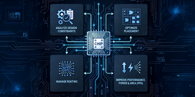
Their work typically involves analysing design constraints, optimising layout placement, managing routing of interconnections, and ensuring that the chip design meets performance, power, and area requirements.
Physical Design engineers collaborate with digital designers, verification engineers, and other semiconductor specialists to ensure that the final chip design is both functional and manufacturable.
This role plays an essential part in transforming digital circuit designs into real silicon chips used in electronic devices.
Students with backgrounds in electronics, electrical engineering, or related fields often explore Physical Design as part of their preparation for semiconductor careers.
Those who enjoy understanding how digital designs are implemented as manufacturable chip layouts may find this domain particularly interesting.
Students exploring semiconductor training may also compare domains such as
Physical Design, Design Verification, and Analog Layout to determine which path best aligns with their interests and career goals.
S.I.T. advisors can help students understand these domains and guide them toward the most suitable learning path.
S.I.T supports eligible candidates through structured financial support options designed to make specialised semiconductor training more accessible while maintaining program standards.
These options are offered based on a defined evaluation process to ensure alignment with student readiness and commitment to the training.
Selected candidates may benefit from:
Students admitted under these options undergo the same training structure, curriculum, and internship exposure as other students, ensuring consistency in learning outcomes.
These initiatives are designed to support deserving candidates while maintaining strong training quality and expectations.
Physical Design is the stage of semiconductor design where digital circuit designs are converted into manufacturable chip layouts through processes such as placement, routing, and timing optimisation.
Physical Design engineers typically work with digital design concepts, timing analysis, and semiconductor design tools used for chip implementation.
Physical Design workflows commonly use specialised semiconductor design tools from ecosystems such as Cadence, Synopsys, and Mentor Graphics.
Physical Design remains an important part of semiconductor development because every digital chip design must be implemented and optimised before fabrication.
Engineering graduates with backgrounds in electronics, electrical engineering, or related fields often pursue training in Physical Design to prepare for semiconductor design roles.