About S.I.T. | VLSI Training Institute for Semiconductor Careers

Introduction

Sumedha Institute of Technology (S.I.T.) is a VLSI training institute focused on semiconductor careers. Founded in 2017 in Hyderabad, S.I.T. was established to address the gap between engineering education and the practical requirements of semiconductor roles.

What began as a focused VLSI training initiative has evolved into a structured learning environment that prepares engineers for real-world chip design work. The institute’s approach is built around clarity of concepts, practical application, and exposure to industry-relevant tools and workflows.

S.I.T. works with students at different stages, supporting their transition from foundational understanding to role readiness in a systematic and measurable manner.

8+
Years of Experience
250+
Recruitment Drives
2000+
Alumni
15+
Average Faculty Experience

Our Approach to VLSI Training

img

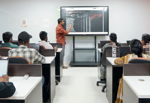
S.I.T. follows a structured training model aligned with how semiconductor roles function in the industry. The focus is on building both conceptual understanding and the ability to apply that knowledge in practical scenarios.

The training approach includes:

  • Concept-driven learning mapped to industry expectations
  • Hands-on exposure to relevant tools and design environments
  • Scenario-based learning through industry-inspired design problems
  • Continuous evaluation to track learning progress
  • Advisor-led guidance to support decision-making
  • AI-powered engineering support for problem solving, debugging, analysis, and automation

This ensures that students are not only completing modules but also developing the capability required to work in VLSI roles.


Explore Courses

Faculty with Industry Experience

S.I.T. believes that effective semiconductor training requires more than theoretical instruction alone.

Many members of the faculty team bring experience from semiconductor and VLSI environments where design, verification, implementation, and engineering problem solving are performed as part of real projects and development activities.

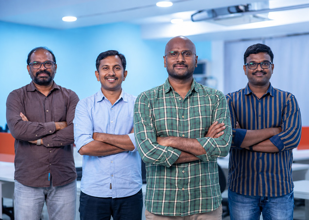
Faculty experience includes work across leading semiconductor and technology organisations such as Intel, NVIDIA, AMD, Synopsys, and other companies within the semiconductor ecosystem.

Their experience helps students gain a deeper understanding of semiconductor workflows, engineering expectations, and the practical considerations involved in chip development.

By combining structured learning with industry perspective, S.I.T. aims to help students develop knowledge that is both technically relevant and professionally applicable.


Meet Our Faculty
img

Industry Exposure and Internship

img

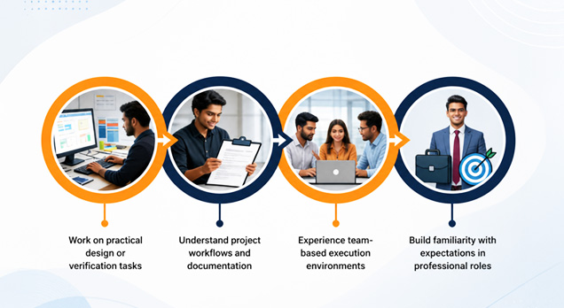
Industry exposure is an integral part of the S.I.T. learning model. Every student undergoes a 6-months internship designed to simulate real working environments within semiconductor projects.

During this phase, students:

  • Work on practical design or verification tasks
  • Understand project workflows and documentation standards
  • Experience team-based execution environments
  • Build familiarity with expectations in professional roles

This structured exposure helps bridge the gap between training and industry requirements, making the transition to employment more practical.

Career Pathways in Semiconductor Domain

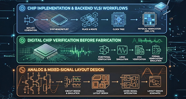
S.I.T. prepares students for specific roles within the semiconductor ecosystem. Training is aligned to clearly defined pathways so that students understand the direction of their learning and the expectations associated with each role.

Common pathways include:

  • Physical Design Engineer
  • Design Verification Engineer
  • Analog Layout Engineer

Students receive guidance in selecting a pathway based on their background, aptitude, and interest. The focus remains on building role-specific capability rather than broad, undefined knowledge.

img

Selection, Evaluation and Support

img

S.I.T. maintains a structured evaluation process to ensure that students are progressing in line with industry expectations. Performance is tracked continuously, and feedback is provided at different stages of the program.

For candidates applying under the Pay After Placement (PAP) model, selection is based on defined criteria. This option is available only for selected candidates and involves an evaluation process before admission.

Support systems include:

  • Periodic assessments and performance reviews
  • Advisor-led mentoring sessions
  • Structured feedback on assignments and progress
  • Interview preparation support

This framework ensures clarity in expectations and consistency in outcomes.


Apply Now

Career Outcomes and Placement Visibility

S.I.T.’s training is aligned to support entry into semiconductor roles. To enable informed decision-making, placement outcomes are documented and presented with clarity.

Instead of relying on broad summary claims, S.I.T. shares recent placements in a structured format. This allows prospective students to understand:

  • The types of roles students move into
  • How training aligns with job responsibilities
  • Typical transition paths from training to employment

This approach provides visibility into outcomes through real examples, helping applicants assess relevance based on their own background and goals.

Detailed placement information is available on the dedicated placements page.


View Placements
img

Placement Highlights

Prasanna Lakshmi

Capgemini

Manohar Reddy

AMD

Sasi Kala

HCL

Manohar

Wipro

Kamala

Digicomm Semiconductor

Kusuma

Chipex Technologies

Partnerships and Ecosystem

img

S.I.T. operates within a broader ecosystem that includes industry interactions and access to relevant tools and platforms. The institute has engaged with over 270 companies across hiring, exposure, and collaboration.

Access to global design tools and evolving industry practices ensures that training remains aligned with current expectations. These interactions are used to strengthen learning relevance and improve career readiness.

Our Vision

S.I.T. aims to contribute to the semiconductor ecosystem by preparing engineers who are capable of working on real-world design and verification challenges.

The institute focuses on:

  • Bridging the gap between academic learning and industry requirements
  • Enabling structured entry into semiconductor careers
  • Building long-term capability in VLSI domains

This vision guides how programs are designed and delivered.

img

Who Should Consider S.I.T.

img

S.I.T. is designed for individuals who are looking to build a career in semiconductor domains through structured training.

This includes:

  • Final-year ECE and EEE students
  • Recent graduates (0–2 years) seeking entry into VLSI roles
  • Early-career professionals exploring a transition into semiconductor domains

The programs are structured to support both foundational learning and career transition.

Frequently Asked Questions

S.I.T. specializes in VLSI training aligned to semiconductor careers, with a focus on role-based learning and industry readiness.

Yes, all students undergo a structured 6-months internship as part of the training.

PAP is available for selected candidates based on a defined evaluation process. It is not applicable to all applicants.

No prior deep VLSI knowledge is required. Programs are designed to build understanding from foundational to advanced levels.

S.I.T. shares recent placements in a structured format to provide visibility into career transitions. This helps applicants understand role alignment and outcomes through real examples.